TESCAN
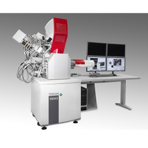
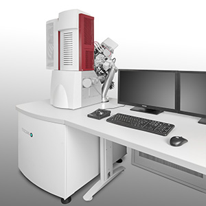
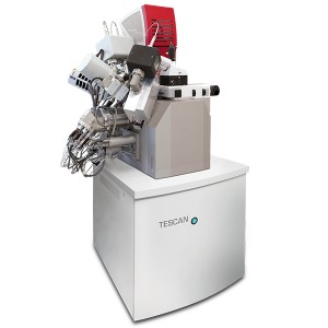
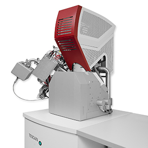
TESCAN, is a Czech joint-stock company focused on the research, development and manufacturing of scientific instruments and laboratory equipment such as:
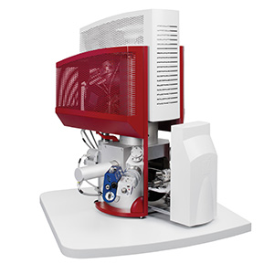
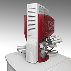
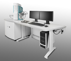
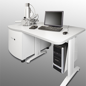
- Scanning electron microscopes
- Focused ion beam systems
- Supplementary accessories for SEMs
- Special vacuum chambers and custom systems
- Detection systems
- Scientific hardware and software development
TESCAN was established in the summer of 1991 by a group of 5 former R&D and service engineers from a now defunct producer of electron microscopes, Tesla Brno. TESCAN has changed from an almost family business into a company with a distinct structure that is subordinate to the main objectives of the company i.e. to the development, manufacturing and sales of scanning electron microscopes.
In August 2013, TESCAN merged with Orsay Physics, a world leader in customised focused ion beam and electron beam technology, forming TESAN ORSAY Holding. This followed on from 2007, when Orsay Physics had been TESCAN’s sole supplier of ion beam technology. The co-operation lead to the development of a number of FIB-SEM workstations and the FERA Xe-plasma FIB-SEM, while the merger will allow both organisations to grow further and better serve their customers and develop their electron and ion beam technologies.
TESCAN Today
TESCAN is a global supplier of scanning electron microscopes and focused ion beam systems used for research and manufacturing in the fields of the semiconductor, automotive and aerospace industries, biotechnology, nanomaterials, metallurgy, education and forensic science. The company is located in Brno, the Czech Republic, a traditional centre of charged particle optics research that includes over sixty years of work in the design and production of electron microscopes. During the 22 years of its existence, the TESCAN brand has built a reputation for quality, reliability, and innovation, with over 1500 SEMs installed in more than 60 countries.
Currently, more than 200 employees work in a modern manufacturing facility that includes machine shops, equipment for the production of electronic components, assembly rooms, clean rooms for the assembly of UHV systems and components, facilities for system integration, research and application laboratories, offices, etc. TESCANs sales and service network covers countries all over the world. The team of experienced sales representatives and a well-trained service staff is able to ensure fast service and excellent customer support as well as detailed product information. Finally, the establishment of the subsidiary TESCAN China and the acquisition of TESCAN USA Inc. as well as TESCANs rapidly increasing worldwide sales, provide evidence of TESCANs robust and stable business growth.
TESCAN for the Future
TESCAN is building its reputation in the field of design, manufacture and sales of SEMs and system solutions for various
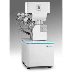
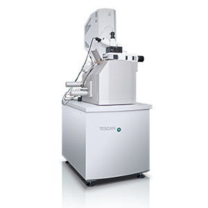
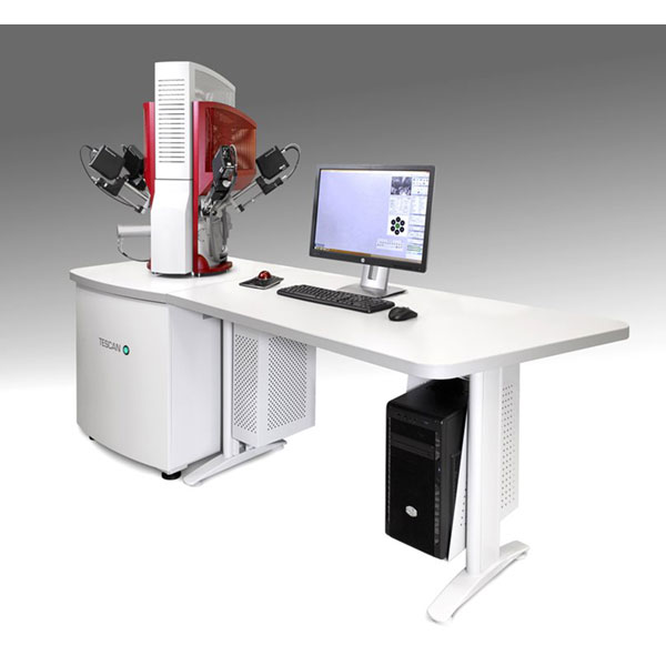
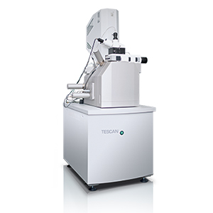
applications. Its product range includes thermal emission systems (VEGA), LaB6 systems (VEGA), field emission systems (MIRA), dual beam systems (LYRA / VELA) and world class innovation: a dual beam system integrating TESCANs FEG-SEM technology with Focused Ion Beam columns utilizing novel plasma ion sources (FERA). Furthermore, TESCAN offers special solutions tailored to customers needs, such as extra-large SEM chambers with an extremely large observable area or instruments modified for hot cells to examine radioactive materials. TESCANs continuous participation in top research projects and close co-operation with the leading European universities and research institutions, as well as partnerships with innovative companies in the field of surface analysis instrumentation, nanotechnologies, life sciences and advanced materials, have resulted in great scientific and technical achievements.
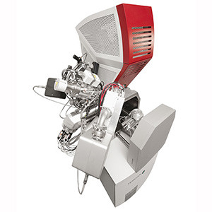
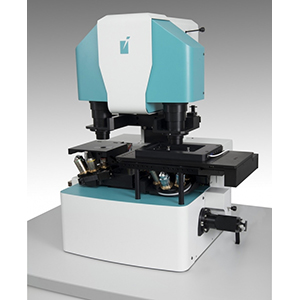
In the framework of the EC project FIBLYS, a unique Multi-Nano-Tool integrating three sources of surface atom excitation has been designed and successfully completed: electrons (SEM), ions (FIB) and SPM probes. A complex set of detectors and supplementary accessories enables surface modification, in-situ testing and the detection of almost all the useful signals originating from the interaction between the surface atoms and these excitation sources. Devices such as a Gas Injection System, Nano-Manipulators and Nano-Indentors, various loading stages (heating, cooling, bending, ripping, etc.), a comprehensive range of detectors (SE, BSE, In-lens SE, In-lens BSE, TE, CL and colour CL, EDX, WDX, EBSD) and special tools such as Time-of-Flight Mass Spectrometer or EBIC can be used for the creation of nanostructures, their visualisation and complete analysis and testing their features. Sophisticated automated procedures and dedicated software also enable three-dimensional investigation and 3D visualisation in several modes (Nano-Tomography).

