AXT Bring Unique Rapid Nanofabrication Technology to Australia
AXT are proud to be able to bring another exciting new technology to Australia and New Zealand. With the recent signing of a distribution agreement with SwissLitho, they will be making their unique rapid nanofabrication technology available to local researchers. This will help to keep them at the cutting edge by ensuring that they have the most up-to-date tools available for nanotechnology development.
Nanofabricated devices are used in a wide range of research and real world applications. These include nanooptics, nanoelectronics, plasmonics, biology, nanofluidics, MEMS and quantum computing to name but a few. The growth of these fields relies on the fabrication of high precision nanopatterns, nanostructures and prototypes with features smaller than 100 nm, which is where the SwissLitho NanoFrazor Explore excels.
The thermal Probe Scanning Lithography (t-SPL) technology was developed by IBM and commercialized by SwissLitho. The NanoFrazor Explore can produce 2D & 3D nanostructures in a single step and operate in ambient conditions and has no requirement for high voltage. This has distinct advantages over electron beam lithography (EBL) systems which have been around for nearly 50 years. EBL systems are typically bulky and require ultra high vacuum environments with high voltage supplies.
SwissLithos technology uses an extremely sharp tip that is similar to an AFM tip that heats a very localised area resulting in decomposition, effectively machining the surface of the resist material. The tip that has a radius better than 5 nm is thus able to create a high resolution nanopattern, for example sub-10 nm half-pitch lines were demonstrated.
Another advantage of the NanoFrazor is its ability to operate in Close Loop Lithography mode. This enables you to simultaneously pattern and measure your sample, providing instantaneous feedback on your patterning process. The patterning depth can be controlled with nm accuracy, which enables direct patterning of 3D nanostructures in a single step. It also eliminates the need for subsequent imaging of your sample after patterning which speeds your workflow and research. Furthermore, new stitching and overlay methods have been developed that achieve sub-5nm accuracy without the use of artificial marker structures.
The heated tip in the lithography process does not deposit charged particles like electrons or ions into the sample. For dedicated nanoelectronic devices this can result in superior device performance.
Despite the high precision nature of the instrument, it is easy to use thanks to a smart software architecture and user-friendly graphical user interface that simplifies many complex functions. This enables high-resolution nanometer sized geometries to be quickly prototyped and will help researchers push past the limits of EBL.
AXTs Managing Director Richard Trett commented after the signing of the agreement, we pride ourselves in being able to bring new technologies into Australia and into the hands of our researchers. It is imperative that our researchers have the tools they require to keep our country at the forefront of science and technology. SwissLithos NanoFrazor systems certainly fit the bill and have many advantages over more conventional technologies. Apart from the technical advantages, the attractive pricing and low running costs of these systems should help the technology become more widely adopted.
Felix Holzner CEO from SwissLitho went further to say, we are pleased to have partnered with AXT who have an enviable track record of working with young and innovative companies such as ours. We have identified the potential of the Australian market and feel that working with AXT is a perfect match for us.
AXT will be promoting the NanoFrazor Explore at the upcoming ICONN (International Conference on Nanoscience and Nanotechnology) that will take place in Canberra from February 7 to 11.
Posted January 18, 2016
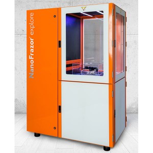
The NanoFrazor Explore thermal Scanning Probe Lithography (t-SPL) system for rapid prototyping nanopatterns and nanostructures.


